Doubling the Resolution of Solid Immersion Microscopes: Update
Posted : 8 years, 10 months ago
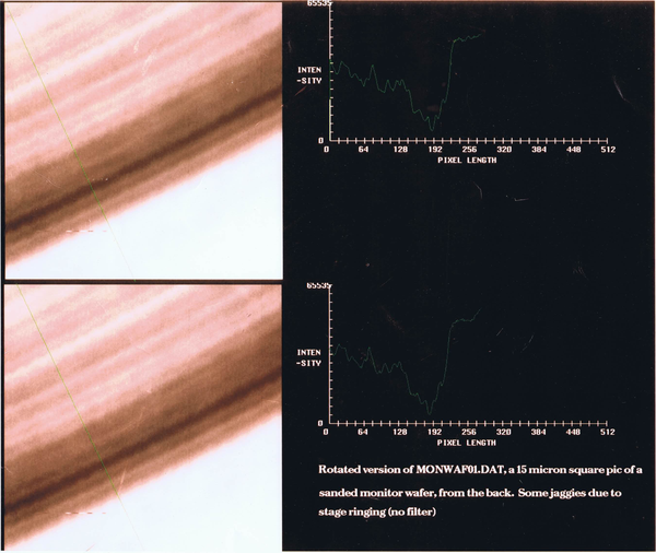
This is a very exciting development, in cooperation with a semiconductor equipment manufacturer. Back in 1989, my colleagues and I started working on a contact-lens microscope for looking into the interior of silicon chips through the back surface. In 1992 I took a picture (shown above) at a numerical aperture of 2.5, with resolution equivalent to NA 3.5 due to a confocal design.
The combination of this with my thesis work on doubling conventional microscope resolution via heterodyne interferometry and digital filtering was going to allow us to take images at an equivalent numerical aperture of 6.4. I never got to build the full scale system.
Now, over 20 years later, I finally get to do it for real. I'm designing and prototyping a microscope to work at NA 6.4, which will have resolution on the order of 15 nm (10%-90% rise). That's pretty cool stuff for a visible-light microscope, and if it works, it should give me bragging rights for a long, long time.
Recent Posts
-
Featured Product: LA-22 Low Noise Lab Amplifier
-
 "Super-Regenerative Receivers" by J. R. Whitehead
 -
Temperature Control 1: Simple Control Theory
-
A High-Performance Time Domain Reflectometer
-
Product Announcement: QL03 Photoreceiver
Archive
2026
- January (1)
2025
2023
- May (1)
2021
- January (3)
2020
2018
2017
2015
2014
2013
2012
2011
Categories
- Design Support Consulting (8)
- Expert Witness Cases (15)
- New Technology (1)
- News (33)
- Products (4)
- SED (16)
- Sensitive Design (6)
- Ultrasensitive Instrument Design (27)
Tags
- photon budget (1)
- prototype (1)
- SEM (2)
- microscopy (1)
- microscope (1)
- product (1)
- noise (2)
- ultraquiet (1)
- thermoelectric cooler (1)
- Jim Thompson (1)
- analog-innovationscom (1)
- analog (2)
- ic design (1)
- scielectronicsdesign (1)
- website archive (1)
- MC4044 (1)
- MC1530 (1)
- SiPm (2)
- MPPC (2)
- PMT (1)
- Photomultiplier (2)
- frontend (1)
- module (2)
- hammamatsu (1)
- APD (2)
- SPAD (2)